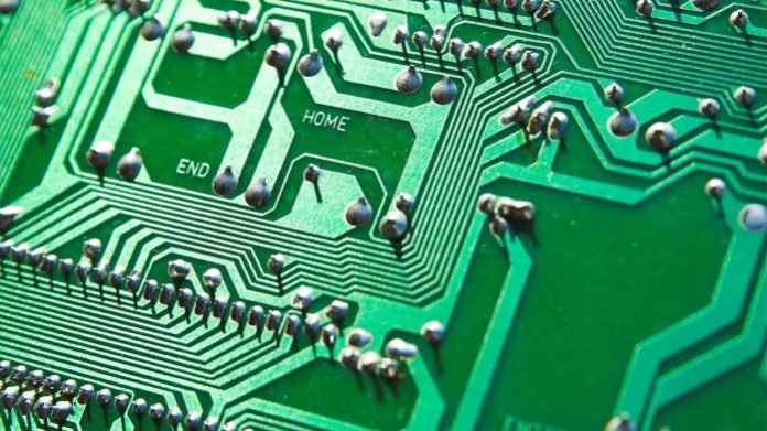
Have you ever watched an old movie and marveled at the gigantic size of old cell phones and computers?
As predicted by Moore’s law, the number of transistors that can fit onto one computer chip has been doubling almost every year, allowing electronics to get smaller and smaller. Devices from just a few years ago can seem ridiculously bulky.
But even Gordon Moore, the co-founder of Intel and author of Moore’s law, knows we’re approaching the limit. As transistors begin reaching the same size scales as atoms, electronics no longer behave the way we expect them to. There’s only so far we can go with conventional transistor-based technology.
Now, researchers from the University of Alberta, led by Professor Robert Wolkow, have found a way to fix imperfections on a silicon chip with atomic-scale precision – a discovery that could propel us beyond the transistor age.
Heating up
Transistors are the major building blocks of your computer’s brain – by controlling the flow of electrons through a circuit, transistors essentially control your computer’s decisions. Transistor-based computer circuitry has been effective for decades, but that doesn’t mean it’s perfect.
Transistors use a lot of energy and, just like an incandescent light-bulb, they heat up. This heating effect is, in fact, the major barrier towards increasing computer speed.
“For the last 15 years or so, “scaling” has failed,” explains Wolkow, who is also the Principal Research Officer at the Nanotechnology Initiative. Transistors got smaller but the power they use did not decrease proportionally, so their density on a chip is limited by heat generation. “This is why clock speed has stopped rising. A computer you bought 8 years ago would have a 1 to 3 GHz clock – so will the one you buy today.”
So how can we overcome these inherent problems?
One radically new approach, called field controlled computing, eliminates transistors altogether. Theoretically, it looks enticing, but it is isn’t very practical yet – early proof of concept work required temperatures around -270°C. New designs based on atomic-scale circuits looked more promising for room temperature operation, but working at the atomic scale comes with its own set of challenges. Imperfections in manufacturing that are forgivable in a bulk material, suddenly become very important.
Big problems at a small scale
Just like transistors, atomic circuits are made from silicon that has had its surface insulated or passivated with hydrogen. The hydrogen atoms essentially act as a barrier so that electrons only go where they’re supposed to go. But there are always a few silicon atoms that get away from the manufacturing process with no hydrogen, forming so-called dangling bonds. These imperfections in the final circuit and can trap electrons, impeding operation. For conventional circuitry a few atomic imperfections won’t make much of a difference in overall performance, but at the atomic scale, a few misplaced atoms can have a huge impact. The required level of perfection in the fabrication process has been unattainable, until now.
In the recent paper published in ACS Nano, Wolkow’s group describes “atomic white-out”: a method of selectively replacing the missing hydrogen atoms on a silicon surface, essentially erasing any imperfections. Now, with nothing impeding their performance, atomic-scale circuits are within reach.
Microscopy for manipulation
To manipulate single hydrogen atoms on the silicon surface, Wolkow’s team used atomic force microscopy (AFM). Although it’s called microscopy, AFM can measure forces and perform manipulations in addition to imaging.
The process relies on the sensing of tiny forces, essentially electrons repelling each other, between the tip of an AFM probe and a surface. For imaging, the reaction of the probe to these forces as you scan along a surface essentially provides a topographical map of that surface. In the case of manipulation, applying a localized electronic excitation at the AFM probe tip can instead cause an atom to detach from the surface and attach to the tip. Think of it like one of those arcade claw games where the claw is the AFM probe and the hydrogen atoms are the prizes.
When the tip, now charged with a hydrogen atom, is brought close to a dangling bond, it forms a connection. By doing this, Wolkow’s team was able to demonstrate creation and destruction of dangling bonds with atomic precision. This ability to correct mistakes would allow for manufacturing of perfectly identical circuit elements.
“Perfection of structures… means like units will have virtually zero dispersion of qualities – and that in turn – leads to cleaner operation,” explains Wolkow.
He likens it to the construction of a series of doors: if your manufacturing process is not perfect, you may not be sure how big the door will turn out to be, so you make all the door frames big enough to accommodate the largest possible size. But this means that some doors might end up with huge gaps all around. Creating perfect transistors is like creating perfect doors – you always know exactly what they will be like, so you won’t have to make allowances for imperfection and can thus improve overall performance.
Going atomic
Wolkow has been planning and progressing towards atomic circuitry for almost 30 years.
“[This] paper is a culmination of a life’s work. It’s a super exciting time,” he says.
The new technology is being commercialized in a spin-off company, Quantum Silicon, where Wolkow is the Chief Technology Officer.
“The new circuitry will be the smallest, fastest, greenest (lowest power and material consuming) circuitry ever. That’s why it will be revolutionary.”


