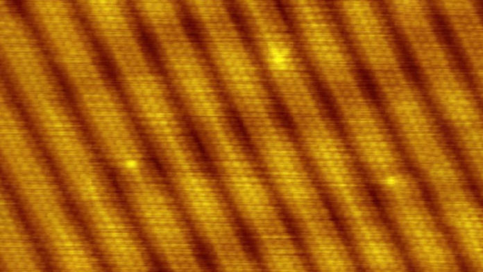
Microscopes can peer all the way down to the atomic level, but understanding behaviour at these ultra-small scales also requires instruments that can visualize the ultra-fast.
“Just like how new telescopes allow scientists to explore further into space, this new instrument will allow us to explore these very fast processes that happen all the time, but on nanometre-length scale dimensions, and no one else has that capability,” said Frank Hegmann, professor of physics at the University of Alberta, in a press release.
We can see individual atoms thanks to scanning tunneling microscopy (STM), an innovation that netted the 1986 Nobel Prize in Physics. STM uses an extremely sharp metal tip that scans over the surface of a material, and while individual atoms can be visualized this way, the process is slow. Conventional STM also happens at ultra-cold temperatures (near absolute zero) to slow molecular motion to the point where a sharp image can be taken.
Hegmann’s instrument uses ultra-fast laser light pulses, pulsing a trillion times a second to control the movement of the probe tip like an antenna. It’s a coupled strategy called terahertz STM, and it harnesses the spatial resolution of STM at much faster speeds.
The device demonstrates spatial resolution down to 2 nanometres, with a new image in under 500 femtoseconds at normal room temperatures. The ability to scan over surfaces with added speed allows researchers to capture movies of atomic-level phenomena instead of only being able to look at snapshots.
Nanotechnology is a growing field that will benefit from the insights that terahertz STM will provide. From better materials for harvesting solar energy, to smarter design of superconducting devices, researchers will be able to study how they work in a way that has never been possible before. The same instrument will even allow researchers to manipulate materials by using the probe tip to move individual atoms around.
Since publishing this research in Nature Photonics in 2013, terahertz STM is now used in labs worldwide, but Hegmann is continuing to expand the concept by building a device that can probe multiple points on a surface simultaneously.
Being able to watch atomic processes unfold gives unique insight on how they work, and also on how they can be improved. It’s an unprecedented window to these nanoscale worlds that is sure to change the way we view materials across many fields.


